CIES Consortium
Industry-Academic Collaboration
Spintronics LSI Technology
R&D of technologies to automatically design environments for low-energy consumption and highly functional VLSI processors based on non-volatile memory
-
 Research Director
Prof.
Takahiro Hanyu
In order to overcome a power-wall problem in 4x-nm CMOS era and beyond, our R&D project aims to develop nonvolatile (NV)- device-based logic-circuit Intellectual Properties (IPs) and its automated design environment. The actual development items are as follows:
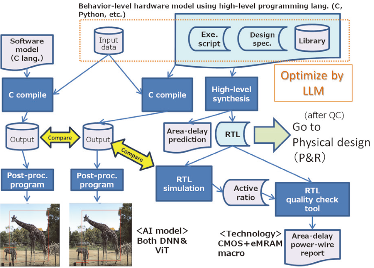
- Development of an automated-design CAD environment for NV-LSIs (cf. Figure right)
We are engaged in the development of an automated CAD environment for low-power and high-performance NV circuits and systems that integrate emerging back-end memory technologies such as MRAM. - Development of a NV-based circuit IPs
We have also been developing logic-circuit IPs (LUTs, NV registers, etc.) for realizing a further energy-efficient/highly functional NV-LSI. - Applications to AI accelerators
As an effective application, we are developing NV-based energy-efficient AI accelerators.
It is expected that the NV-LSI is utilized in a wide variety of applications such as IoT and mobile devices.