CIES Consortium
Industry-Academic Collaboration
LSIs
R&D of technologies to automatically design environments for low-energy consumption and highly functional VLSI processors based on non-volatile memory
-
 Prof.
Prof.
Takahiro Hanyu
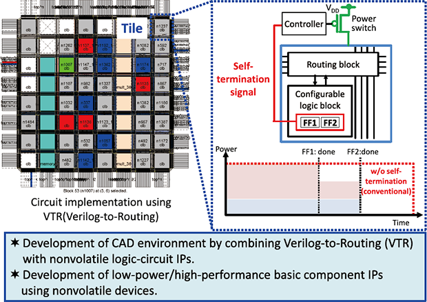
To overcome a power-wall problem in 4x-nm CMOS era and beyond, our R&D project aims to develop nonvolatile (NV)-device-based logic-circuit Intellectual Properties (IPs) and its automatic design environment. Infact, we have been developing a CAD environment for NV field-programmable gate arrays (FPGAs). We have almost established the environment by combining an open-source CAD tool, called Verilog-to-Routing (VTR), with nonvolatile logic-circuit IPs. We have also been developing logic circuit IPs for realizing a further high-speed/low-power NV-FPGA. It is expected that the NV-FPGA is utilized in a wide variety of applications such as IoT and mobile devices.
Design technology of Nonvolatile FPGA