CIES Consortium
Industry-Academic Collaboration
LSIs
R&D of STT-MRAM aimed at developing non-volatile working memory and its manufacturing technologies
-
 Prof.
Prof.
Tetsuo Endoh -
 Prof.
Prof.
Hideo Ohno -
 Prof.
Prof.
Shoji Ikeda
In this R&D project, STT-MRAM and its fabrication technology are researched and developed with combining the spintronics technology and the silicon CMOS technology, in a joint effort between industry and academia. The aim of the project is to accelerate the realization of nonvolatile working memories that will make super low-power electronic systems possible and to contribute to the realization of low carbon society with low-power electronic appliances. The actual development items are as follows:
- Material/device/physical analysis technologies for the magnetic tunnel junctions (MTJs) that have a compatibility for CMOS integrated circuits,
- Unit process and process integration technologies for fabricating the STT-MRAMs,
- Circuit/design/measurement technologies for the STT-MRAMs from the view point of developing stand-alone and embedded memories for logic LSIs.
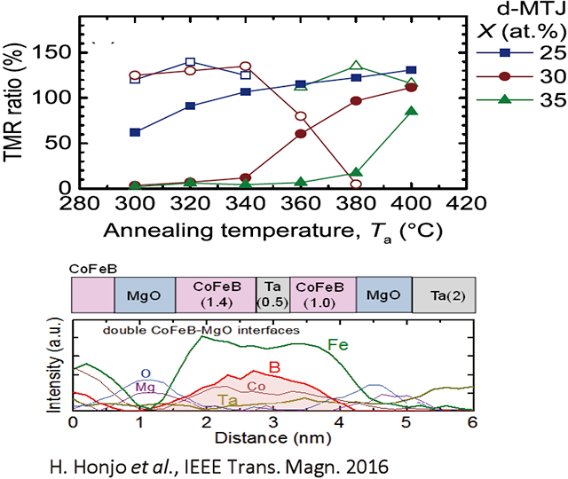
Cause investigation of high annealing tolerance in MTJs with a compatibility for CMOS integrated circuits using 300 mm wafer
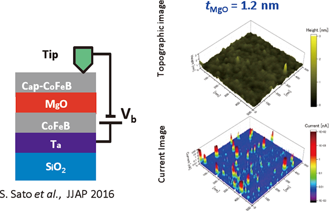
Characterization of tunneling current on MgO tunneling barrier of MTJ by Conductive-AFM
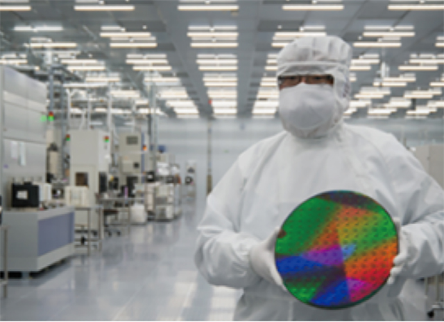
Prototype development environment (the leading-edge clean room and the manufacturing process equipment using 300 mm wafers) at CIES and the prototype 300 mm wafer
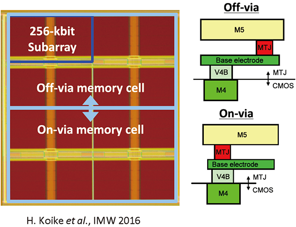
Development of On-via STT-MRAM chips